| CPC H10B 51/40 (2023.02) [G11C 11/2255 (2013.01); G11C 16/08 (2013.01); H01L 23/5226 (2013.01); H10B 43/27 (2023.02); H10B 43/40 (2023.02); H10B 51/20 (2023.02); H10B 43/10 (2023.02); H10B 51/10 (2023.02)] | 20 Claims |
|
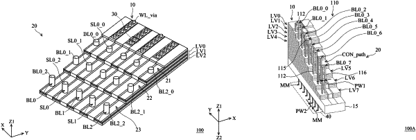
1. A three-dimensional memory, comprising:
a memory cell array comprising a plurality of memory cells formed in a plurality of levels stacked in a first direction;
a first interconnect structure formed on one side of the memory cell array, and comprising:
at least one bit line extending in a second direction that is perpendicular to the first direction, wherein the bit line comprises a plurality of sub-bit lines stacked in the first direction, and each of the sub-bit lines is coupled to the memory cells arranged in a line in the corresponding level of the memory cell array;
a bit line decoder formed under the memory cell array and the first interconnect structure; and
a second interconnect structure configured to connect the bit line to the bit line decoder passing through the first interconnect structure.
|