| CPC H10B 51/20 (2023.02) [G11C 7/18 (2013.01); G11C 11/14 (2013.01); H10B 51/10 (2023.02)] | 20 Claims |
|
1. A method of forming a ferroelectric random access memory (FeRAM) device, the method comprising:
forming a first layer stack and a second layer stack successively over a substrate, wherein each of the first layer stack and the second layer stack has a first dielectric layer and an electrically conductive layer formed over the first dielectric layer;
patterning the first layer stack and the second layer stack, wherein the patterning forms a staircase-shaped region, wherein after the patterning, the first layer stack extends beyond lateral extents of the second layer stack;
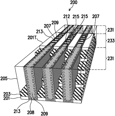
after the patterning, forming a trench that extends through the first layer stack and the second layer stack;
lining sidewalls and a bottom of the trench with a ferroelectric material;
forming a channel material over the ferroelectric material;
filling the trench by forming a dielectric material over the channel material; and
forming a conductive line in the dielectric material, wherein the conductive lines extends through the second layer stack and the first layer stack.
|