| CPC H10B 43/40 (2023.02) [H01L 25/0657 (2013.01); H01L 29/4234 (2013.01); H01L 29/66833 (2013.01); H10B 43/27 (2023.02); H10B 43/35 (2023.02); H10B 43/50 (2023.02)] | 20 Claims |
|
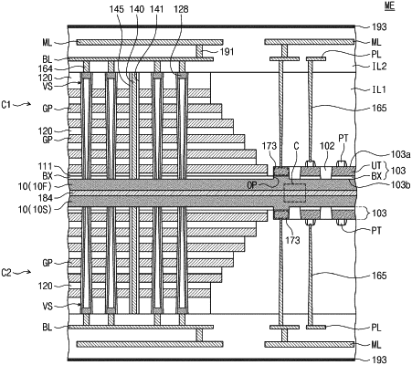
1. A semiconductor memory device comprising:
a first semiconductor chip and a second semiconductor chip, each semiconductor chip of the first semiconductor chip and the second semiconductor chip including
a cell array region, the cell array region including
an electrode structure including a plurality of electrodes sequentially stacked on a body conductive layer, and
a plurality of vertical structures extending through the electrode structure and connected to the body conductive layer, and
a peripheral circuit region, the peripheral circuit region including a residual substrate on the body conductive layer and on which a peripheral transistor is located,
wherein a bottom surface of the body conductive layer of the second semiconductor chip faces a bottom surface of the body conductive layer of the first semiconductor chip,
wherein the residual substrate includes a buried insulation layer in the peripheral circuit region, and the peripheral transistor is disposed on the buried insulation layer.
|