| CPC H10B 43/27 (2023.02) [H01L 21/02532 (2013.01); H01L 21/02636 (2013.01); H01L 21/31111 (2013.01); H01L 21/76802 (2013.01); H01L 21/76831 (2013.01); H01L 21/76877 (2013.01); H01L 23/481 (2013.01); H01L 29/40117 (2019.08); H01L 29/513 (2013.01); H01L 29/518 (2013.01)] | 9 Claims |
|
1. A method for fabricating a memory device, comprising:
providing a substrate;
forming a plurality of conductive layers and a plurality of dielectric layers alternately and horizontally disposed on the substrate;
forming a first dielectric layer over the substrate and on at least one of the plurality of conductive layers;
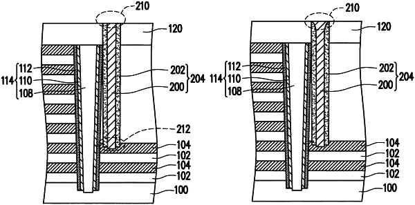
forming, a channel column structure on the substrate and in the plurality of conductive layers and the plurality of dielectric layers, wherein a side wall of the channel column structure is in contact with the plurality of conductive layers; forming a second dielectric layer covering the first dielectric layer directly; and
forming, in the first and second dielectric layers, a conductive column structure adjacent to the channel column structure, wherein the conductive column structure comprises a liner insulating layer as a shell layer, and the conductive column structure is in direct contact with predetermined one of the plurality of conductive layers, and the liner insulating layer of the conductive column structure is in physically direct contact with the channel column structure;
wherein the step of forming the conductive column structure comprises:
forming, in the first and second dielectric layers, a columnar recess extending to the predetermined one of the plurality of conductive layers;
forming the liner insulating layer on a side wall of the columnar recess; and
filling the columnar recess with a conductive material to form a conductive central column in contact with the predetermined one of the plurality of conductive layers, wherein the liner insulating layer covers the conductive material and also isolates the conductive material from the channel column structure.
|