| CPC H10B 43/27 (2023.02) [H10B 41/10 (2023.02); H10B 41/27 (2023.02); H10B 41/35 (2023.02); H10B 43/10 (2023.02); H10B 43/35 (2023.02)] | 18 Claims |

|
1. A three-dimensional memory device, comprising:
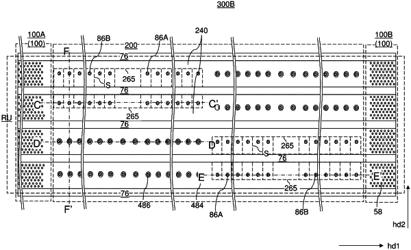
alternating stacks of insulating layers and electrically conductive layers, wherein each of the alternating stacks laterally extends along a first horizontal direction through a first memory array region and a second memory array region that are laterally spaced apart by an inter-array region, wherein a subset of the electrically conductive layers is present within each of the first memory array region, the second memory array region, and the inter-array region as respective continuous layers, wherein the second memory array region is laterally spaced from the first memory array region along the first horizontal direction, and each electrically conductive layer within the subset of the electrically conductive layers comprises a respective strip portion that laterally extends along the first horizontal direction between the first memory array region and the second memory array region, and wherein each of the alternating stacks includes a set of stepped surfaces in the inter-array region;
retro-stepped dielectric material portions overlying a respective set of stepped surfaces of the alternating stacks; and
memory stack structures vertically extending through a respective one of the alternating stacks and located within the first memory array region and the second memory array region,
wherein:
the first memory array region has a first length along the first horizontal direction;
the second memory array region has a second length along the first horizontal direction that is less than the first length;
one of the alternating stacks comprises a vertical stack of a first-tier alternating stack of first insulating layers and first electrically conductive layers and a second-tier alternating stack of second insulating layers and second electrically conductive layers that overlie the first-tier alternating stack;
the retro-stepped dielectric material portions comprise contiguous combinations of a first-tier retro-stepped dielectric material portion contacting the first-tier alternating stack and a second-tier retro-stepped dielectric material portion contacting the second-tier alternating stack;
the first-tier retro-stepped dielectric material portion has a first tapered sidewall laterally extending along the first horizontal direction and vertically extending from a bottommost surface of a respective first-tier alternating stack to a topmost surface of the respective first-tier alternating stack;
the second-tier retro-stepped dielectric material portion has a second tapered sidewall laterally extending along the first horizontal direction and vertically extending from a bottommost surface of a respective second-tier alternating stack to a topmost surface of the respective second-tier alternating stack, wherein a top surface of the first-tier retro-stepped dielectric material portion has a first width along a second horizontal direction that is perpendicular to the first horizontal direction greater than a second width of a bottom surface of the second-tier retro-stepped dielectric material portion along the second horizontal direction; and
a top edge of the first tapered sidewall that is parallel to the first horizontal direction is connected to a bottom edge of the second tapered sidewall that is parallel to the first horizontal direction by a horizontal surface segment of a bottommost surface of the second-tier alternating stack that has a width along the second horizontal direction that equals a difference between the first width and the second width, and the horizontal surface segment of a bottommost surface of the second-tier alternating stack directly contacts a surface segment of the top surface of the first-tier retro-stepped dielectric material portion.
|