| CPC H10B 43/27 (2023.02) [H01L 21/0337 (2013.01); H01L 29/40117 (2019.08); H10B 43/10 (2023.02); H10B 43/35 (2023.02); H01L 23/53295 (2013.01)] | 9 Claims |
|
1. A three-dimensional (3D) memory device, comprising:
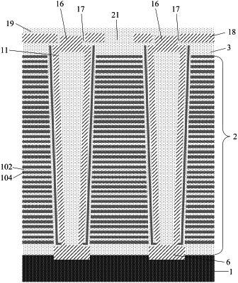
an alternating layer stack on a substrate, wherein the alternating layer stack comprises conductive/dielectric layer pairs stacked in a vertical direction, and wherein each conductive/dielectric layer pair comprises a dielectric layer and a conductive layer;
a first insulating layer on the alternating layer stack, wherein a thickness of the first insulating layer is larger than a thickness of the dielectric layer;
a pair of slits penetrating the alternating layer stack, wherein the pair of slits is extended in a parallel along a first lateral direction;
a plurality of channel holes extending through the alternating layer stack and the first insulating layer;
a channel structure in each channel hole, wherein the channel structure comprises: an epitaxial layer on a bottom of the channel hole, a functional layer on a sidewall of the channel hole, a channel layer covering a sidewall of the functional layer, and a filling structure covering a sidewall of the channel layer and filling the channel hole, and wherein the channel layer comprises a polysilicon layer;
a channel column structure on the channel structure in each channel hole, wherein an upper portion of the channel column structure has a first diameter that is less than a second diameter of a lower portion of the channel column structure;
a top selective gate structure on the first insulating layer, wherein the top selective gate structure is between neighboring channel column structures, wherein the top selective gate structure comprises a polysilicon layer substantially the same as the channel layer, and wherein a thickness of the top selective gate structure is larger than a thickness of the conductive layer;
a second insulating layer between the top selective gate structure and the channel column structure, wherein the second insulating layer comprises an L-type structure, wherein the second insulating layer is disposed on the first insulating layer and wherein the second insulating layer is in contact with a side surface of the channel column structure in the vertical direction;
a third insulating layer on a top surface of the top selective gate structure; and
a top selective gate cut extending through the top selective gate structure and the third insulating layer, wherein:
the top selective gate cut extends partially through the first insulating layer,
a first surface of the top selective gate cut is parallel to a second surface of the top selective gate cut,
a width between the first surface and the second surface is uniform along a second lateral direction perpendicular to the first lateral direction,
the top selective gate cut has a wavy shape extending along a second lateral direction perpendicular to the first lateral direction,
a number N of rows of channel holes are located between the pair of slits, each row of channel holes are arranged staggered with adjacent row of channel holes, and N is an even number that larger than 2, and
the top selective gate cut is located between number N/2 row of channel holes and number N/2+1 row of channel holes.
|