US 11,991,879 B2
Semiconductor device
Yoo-cheol Shin, Hwaseong-si (KR); Young-woo Park, Hwasung (KR); and Jae-duk Lee, Seongnam-si (KR)
Assigned to Samsung Electronics Co., Ltd., (KR)
Filed by SAMSUNG ELECTRONICS CO., LTD., Suwon-si (KR)
Filed on Jan. 22, 2021, as Appl. No. 17/155,441.
Application 17/155,441 is a continuation of application No. 16/844,064, filed on Apr. 9, 2020, granted, now 10,903,226.
Application 16/844,064 is a continuation of application No. 16/396,027, filed on Apr. 26, 2019, granted, now 10,644,019, issued on May 5, 2020.
Application 16/396,027 is a continuation of application No. 15/869,888, filed on Jan. 12, 2018, granted, now 10,381,370, issued on Aug. 13, 2019.
Application 15/869,888 is a continuation of application No. 15/018,477, filed on Feb. 8, 2016, granted, now 9,905,570, issued on Feb. 27, 2018.
Application 15/018,477 is a continuation of application No. 14/534,352, filed on Nov. 6, 2014, granted, now 9,431,415, issued on Aug. 30, 2016.
Claims priority of application No. 10-2013-0135837 (KR), filed on Nov. 8, 2013.
Prior Publication US 2021/0175244 A1, Jun. 10, 2021
Int. Cl. H01L 27/11578 (2017.01); H01L 29/66 (2006.01); H01L 29/788 (2006.01); H01L 29/792 (2006.01); H10B 41/20 (2023.01); H10B 41/27 (2023.01); H10B 41/40 (2023.01); H10B 43/20 (2023.01); H10B 43/27 (2023.01); H10B 43/35 (2023.01); H10B 43/40 (2023.01)
CPC H10B 43/20 (2023.02) [H01L 29/66825 (2013.01); H01L 29/66833 (2013.01); H01L 29/7889 (2013.01); H01L 29/7926 (2013.01); H10B 41/20 (2023.02); H10B 41/27 (2023.02); H10B 41/40 (2023.02); H10B 43/27 (2023.02); H10B 43/35 (2023.02); H10B 43/40 (2023.02)] 11 Claims
OG exemplary drawing
 
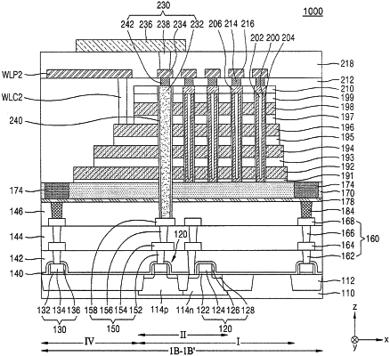
1. A semiconductor device, comprising:
a periphery circuit structure on a lower substrate;
a periphery circuit wiring layer connected to the periphery circuit structure;
an upper substrate on the periphery circuit structure and the periphery circuit wiring layer;
a cell array region and a pad region on the upper substrate, the pad region being adjacent to the cell array region, and the cell array region including a stacked structure in which gate electrodes and insulating layers are alternately arranged in a first direction perpendicular to a top surface of the upper substrate;
channel structures penetrating the stacked structure in the cell array region, the channel structures contacting the upper substrate; and
a through contact penetrating the stacked structure in the cell array region and the upper substrate, the through contact being connected to the periphery circuit wiring layer.