| CPC H10B 41/43 (2023.02) [H01L 29/66825 (2013.01); H01L 29/788 (2013.01); H10B 41/10 (2023.02); H10B 41/44 (2023.02)] | 15 Claims |
|
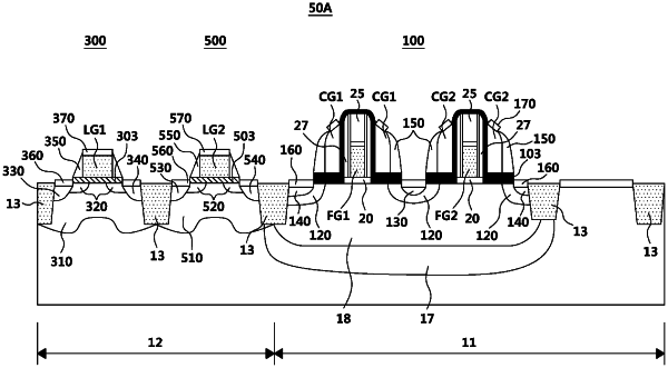
1. A manufacturing method of a semiconductor device, the method comprising:
providing a cell region and a logic region on a substrate;
forming a gate stack comprising a first hard mask pattern and having a first height on the cell region;
forming a control gate insulating layer on the cell region and the gate stack;
forming a logic gate insulating layer on the logic region;
forming a conductive film on the control gate insulating layer and the logic gate insulating layer, the conductive film comprising a first portion and a second portion overlapping the control gate insulating layer and the logic gate insulating layer, respectively;
forming a second hard mask pattern on the second portion of the conductive film;
performing an etch-back process on the conductive film using the first and second hard mask patterns to simultaneously form a spacer-shaped control gate in the cell region and a logic gate in the logic region;
forming a first source region and a first drain region on both sides of the control gate electrode, respectively; and
forming a second source region and a second drain region on both sides of the logic gate electrode, respectively.
|