| CPC H10B 12/50 (2023.02) [H01L 27/0924 (2013.01); H01L 29/0847 (2013.01); H01L 29/167 (2013.01); H01L 29/42368 (2013.01); H01L 29/51 (2013.01); H01L 29/66795 (2013.01); H01L 29/7851 (2013.01); H10B 12/09 (2023.02)] | 17 Claims |

|
1. DRAM circuitry comprising:
a memory array comprising memory cells individually comprising a transistor and a charge-storage device, the transistors individually comprising two source/drain regions having a gate there-between that is part of one of multiple wordlines of the memory array, one of the source/drain regions being electrically coupled to one of the charge-storage devices, the other of the source/drain regions being electrically coupled to one of multiple sense lines of the memory array;
peripheral circuitry comprising wordline-driver transistors having gates which individually comprise one of the wordlines and comprising sense-line-amplifier transistors having gates which individually comprise one of the sense lines;
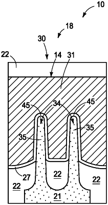
the sense-line-amplifier transistors and the wordline-driver transistors individually being a finFET having at least one fin comprising a channel region of the respective finFET, the sense-line-amplifier transistors and the wordline-driver transistors individually comprising two source/drain regions that individually comprise conductively-doped epitaxial semiconductor material that is adjacent one of two laterally-opposing sides of the at least one fin in a vertical cross-section; and
the finFETs of the sense-line-amplifer transistors and the finFETs of the wordline-driver transistors individually have two and only two channel-region fins along a vertical line through the individual finFET gate and that bisects channel length of the individual finFET.
|