| CPC H10B 12/482 (2023.02) | 14 Claims |

|
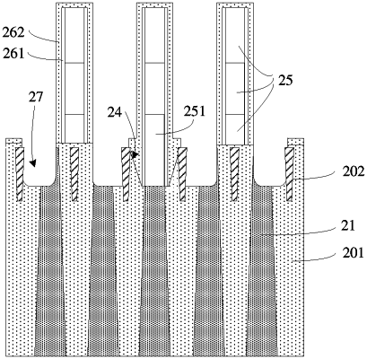
1. A method for forming a semiconductor structure, comprising:
providing active areas and first isolation structures which are disposed at intervals;
forming second isolation structures located between adjacent active areas, top surfaces of the second isolation structures being higher than or flush with top surfaces of the active areas;
forming a mask layer, pattern openings of the mask layer exposing part of the top surfaces of the active areas, and the second isolation structures being located at two opposite sides of part of the active areas;
etching the part of the active areas exposed by the pattern openings and part of the first isolation structures to form intermediate grooves; and
forming bit line structures electrically connected to the top surfaces of the active areas exposed by the intermediate grooves.
|