| CPC H10B 12/315 (2023.02) [H10B 12/0335 (2023.02); H10B 12/34 (2023.02); H10B 12/482 (2023.02)] | 17 Claims |
|
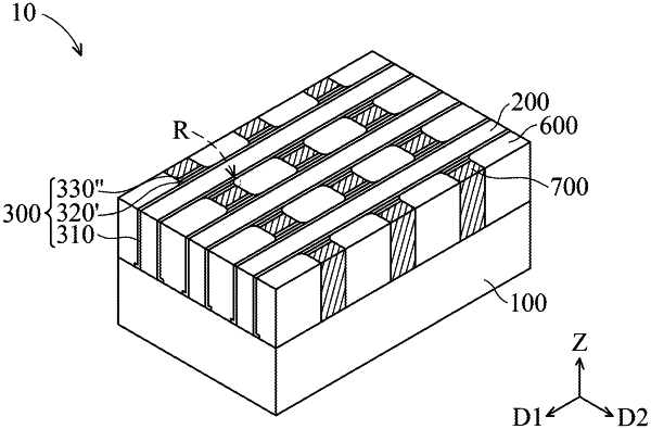
1. A semiconductor memory structure, comprising:
a substrate;
a bit line disposed on the substrate, wherein the bit line extends along a first direction;
a dielectric liner disposed on a side of the bit line, wherein the dielectric liner comprises:
a first nitride liner disposed on a sidewall of the bit line;
an oxide liner disposed on a sidewall of the first nitride liner; and
a second nitride liner disposed on a sidewall of the oxide liner, wherein in the first direction, the oxide liner and the second nitride liner are disposed discontinuously and the oxide liner is longer than the second nitride liner;
a capacitor contact disposed on the substrate, wherein in a second direction perpendicular to the first direction, the capacitor contact is spaced apart from the bit line by the first nitride liner, the oxide liner, and the second nitride liner; and
a filler disposed on the substrate, wherein in the second direction, a width of the filler is greater than a width of the capacitor contact, wherein in the second direction, a side of the filler is spaced apart from the bit line by the first nitride liner.
|
|
5. A method for forming a semiconductor memory structure, comprising:
providing a substrate;
forming bit lines on the substrate, wherein the bit lines extend along a first direction;
forming a dielectric liner on sidewalls of the bit lines, wherein the step of forming the dielectric liner comprises:
forming a first nitride liner on sidewalls of the bit lines;
forming an oxide liner on sidewalls of the first nitride liner; and
forming a second nitride liner on sidewalls of the oxide liner;
forming a dielectric material layer between the bit lines;
forming an opening in the dielectric material layer, wherein sidewalls of the opening expose a portion of the second nitride liner;
along the sidewalls of the opening, laterally removing a portion of the second nitride liner until the oxide liner is exposed;
along the sidewalls of the opening, laterally removing a portion of the oxide liner until the first nitride liner is exposed after the step of laterally removing the portion of the second nitride liner, wherein in the first direction, the remaining second nitride liner and the remaining oxide liner are discontinuous and the remaining oxide liner is longer than the remaining second nitride liner;
forming a filler in the opening; and
replacing the remaining dielectric material layer with a capacitor contact.
|