| CPC H10B 12/30 (2023.02) [H10B 12/482 (2023.02)] | 18 Claims |
|
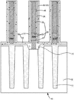
1. A semiconductor structure, comprising:
a substrate, a groove being set in the substrate;
a bit line, a bottom end of the bit line being set in the groove; and
a first isolation layer, the first isolation layer being at least partially set on a sidewall of the bit line, and the first isolation layer being in direct contact with the bit line,
wherein the groove is filled with the first isolation layer;
wherein the first isolation layer comprises:
a first sidewall isolation section, the first sidewall isolation section being set on the sidewall of the bit line and filling the groove; and
a first horizontal isolation section, the first horizontal isolation section being set on an area of the substrate that is outside of the groove;
wherein the semiconductor structure is manufactured by a method comprising:
providing the substrate with the groove;
forming the bit line on the substrate such that the bottom end of the bit line is located in the groove; and
forming the first isolation layer on the sidewall of the bit line such that the first isolation layer fills up the groove;
wherein forming the first isolation layer comprises:
filling up the groove with a first insulation material, and covering the substrate and the sidewall of the bit line; and
laterally etching the first insulation material to form the first isolation layer.
|