| CPC H10B 12/03 (2023.02) [H10B 12/05 (2023.02); H10B 12/30 (2023.02)] | 18 Claims |
|
1. A method for forming a semiconductor device, the method comprising:
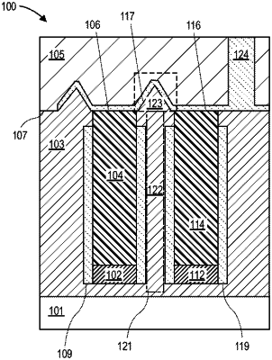
forming a first inter-level dielectric (ILD) layer above a substrate;
forming a first bottom plate of a first capacitor and a second bottom plate of a second capacitor within the first ILD layer, wherein the first bottom plate and the second bottom plate are separated by a first dielectric area in the first ILD layer;
forming a first capacitor dielectric layer adjacent to and above the first bottom plate, and a second capacitor dielectric layer adjacent to and above the second bottom plate;
forming a first top plate of the first capacitor adjacent to and above the first capacitor dielectric layer, and a second top plate of the second capacitor adjacent to and above the second capacitor dielectric layer;
forming a second dielectric area above the first dielectric area and to separate the first top plate and the second top plate, wherein the second dielectric area includes a dielectric material of the first ILD layer;
forming a second ILD layer above the first ILD layer to cover the first top plate, the second top plate, and the second dielectric area; and
forming a conductive segment following a part of a contour of the second dielectric area of the first ILD layer, wherein the conductive segment is to couple the first top plate and the second top plate, and wherein the conductive segment has a non-planar uppermost surface.
|