| CPC H10B 10/125 (2023.02) [H01L 29/0673 (2013.01); H01L 29/42392 (2013.01); H01L 29/7853 (2013.01)] | 20 Claims |
|
1. A method, comprising:
receiving a workpiece that includes:
a substrate having a p-type well and an n-type well,
a first base fin portion over the p-type well and a second base fin over the n-type well, the first base fin portion and the second base fin portion being disposed in an isolation feature disposed over the substrate, and
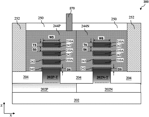
a first semiconductor stack disposed on the first base fin portion and a second semiconductor stack disposed on the second base fin, each of the first semiconductor stack and the second semiconductor stack comprising first semiconductor layers interleaved by second semiconductor layers;
recessing the isolation feature such that a top surface of the isolation feature is lower than a top surface of the first base fin portion by a depth;
forming a dummy gate structure over a channel region of the first semiconductor stack, a channel region of the second semiconductor stack, and the recessed isolation feature;
depositing gate spacers over sidewalls of the dummy gate structure;
after the depositing of the gate spacers, recessing source/drain regions of the first semiconductor stack and the second semiconductor stack to form source/drain trenches;
forming source/drain features in the source/drain trenches;
after the forming of the source/drain features, removing the dummy gate structure from the channel regions of the first semiconductor stack and the second semiconductor stack;
selectively removing the second semiconductor layers to release the first semiconductor layers as suspended channel layers; and
forming a gate structure to wrap around each of the suspended channel layers,
wherein the first semiconductor stack comprises a first width and the second semiconductor stack comprises a second width different from the first width.
|