US 11,991,871 B2
Impedance matching film for radio wave absorber, impedance matching film-attached film for radio wave absorber, radio wave absorber, and laminate for radio wave absorber
Hironobu Machinaga, Osaka (JP); Motoki Haishi, Osaka (JP); Yosuke Nakanishi, Osaka (JP); and Yuuki Takeda, Osaka (JP)
Assigned to NITTO DENKO CORPORATION, Ibaraki (JP)
Appl. No. 17/299,398
Filed by NITTO DENKO CORPORATION, Ibaraki (JP)
PCT Filed Dec. 11, 2019, PCT No. PCT/JP2019/048575
§ 371(c)(1), (2) Date Jun. 3, 2021,
PCT Pub. No. WO2020/122150, PCT Pub. Date Jun. 18, 2020.
Claims priority of application No. 2018-233000 (JP), filed on Dec. 12, 2018.
Prior Publication US 2022/0053675 A1, Feb. 17, 2022
Int. Cl. B32B 15/08 (2006.01); B32B 7/12 (2006.01); H01Q 15/14 (2006.01); H01Q 17/00 (2006.01); H05K 9/00 (2006.01)
CPC H05K 9/0081 (2013.01) [B32B 7/12 (2013.01); B32B 15/08 (2013.01); H01Q 15/141 (2013.01); H01Q 17/008 (2013.01); B32B 2264/102 (2013.01); B32B 2307/202 (2013.01); B32B 2307/204 (2013.01); B32B 2307/212 (2013.01); B32B 2457/00 (2013.01)] 12 Claims
OG exemplary drawing
 
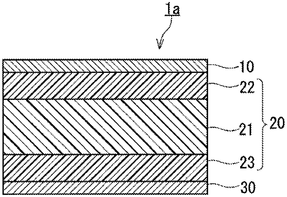
1. An impedance matching film for a radio wave absorber, comprising:
a mixture containing indium oxide and tin oxide and being a main component of the impedance matching film, the mixture having an amorphous structure, wherein
the impedance matching film has a Hall mobility of 5 cm2/(V·s) or more,
the impedance matching film has a thickness of 16 nm or more and less than 100 nm,
the impedance matching film has a sheet resistance of 200 to 800Ω/□ and a content of the tin oxide is 20 mass % or more.