|
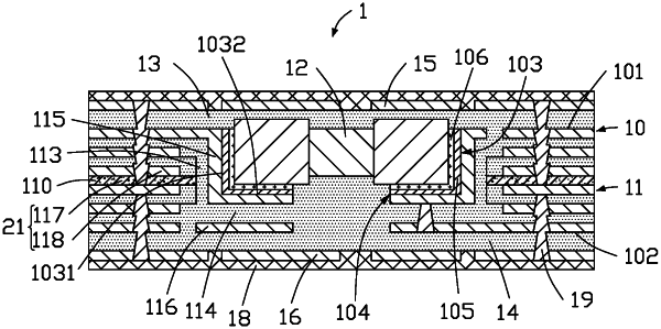
1. An embedded circuit board, comprising: an inner layer assembly, wherein the inner layer assembly comprises a first main portion, a first surface and a second surface are arranged on opposite sides of the first main portion, a first groove is positioned at the first surface, the first groove does not extend to the second surface, a first opening penetrates the second surface and communicates with the first groove; an embedded element, the embedded element is arranged in the first groove; a first insulating element covering the first surface and a surface of the embedded element away from the second surface; and a second insulating element, the second insulating element covers the second surface, the second insulating element extends into the first opening and contact with the embedded element, wherein the first groove comprises a side wall and a bottom wall, the side wall is connected to the first surface and the bottom wall, and the first opening is positioned between the bottom wall and the second surface, and the first opening is filled with the second insulating element, and wherein the inner layer assembly further comprises a first connection layer and a second connection layer, the first connection layer is electrically connected to the second connection layer, the first connection layer is arranged on the bottom wall and the side wall, the first connection layer is electrically connected with the first main portion, and the second connection layer is arranged on a side of the first connection layer adjacent to the embedded element, the second connection layer is electrically connected to the embedded element.
|