| CPC H05K 3/4644 (2013.01) [H05K 1/115 (2013.01)] | 15 Claims |
|
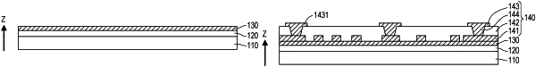
1. A circuit board, comprising:
a substrate;
a build-up circuit structure, disposed on the substrate and comprising:
at least one inner circuit;
at least one dielectric layer, disposed on the at least one inner circuit;
an outer circuit, disposed on the at least one dielectric layer; and
a plurality of conductive vias, penetrating the at least one dielectric layer and electrically connecting the at least one inner circuit and the outer circuit;
a graphene oxide layer and a graphene layer, disposed on the build-up circuit structure at an interval, wherein the graphene oxide layer is disposed in correspondence to the at least one dielectric layer, and the graphene layer is disposed in correspondence to the outer circuit; and
an insulating material layer, disposed on the graphene oxide layer and the graphene layer, wherein the insulating material layer has an opening, and the opening exposes the graphene layer.
|