US 11,991,830 B2
Flexible circuit board assembly, display assembly and display device
Qizhong Chen, Beijing (CN); Bing Ji, Beijing (CN); and Liang Gao, Beijing (CN)
Assigned to Chengdu BOE Optoelectronics Technology Co., Ltd., Sichuan (CN); and BOE Technology Group Co., Ltd., Beijing (CN)
Appl. No. 17/629,586
Filed by Chengdu BOE Optoelectronics Technology Co., Ltd., Sichuan (CN); and BOE Technology Group Co., Ltd., Beijing (CN)
PCT Filed Mar. 26, 2021, PCT No. PCT/CN2021/083382
§ 371(c)(1), (2) Date Jan. 24, 2022,
PCT Pub. No. WO2021/208707, PCT Pub. Date Oct. 21, 2021.
Claims priority of application No. 202010289070.9 (CN), filed on Apr. 14, 2020.
Prior Publication US 2022/0287183 A1, Sep. 8, 2022
Int. Cl. H05K 1/02 (2006.01); H01L 21/78 (2006.01); H01L 23/00 (2006.01); H01L 23/06 (2006.01); H01L 23/28 (2006.01); H01L 23/29 (2006.01); H01L 23/31 (2006.01); H01L 23/538 (2006.01); H01L 23/552 (2006.01); H01L 23/66 (2006.01); H05K 1/18 (2006.01); H05K 7/20 (2006.01); H05K 9/00 (2006.01)
CPC H05K 1/189 (2013.01) [H05K 1/0218 (2013.01); H05K 1/0256 (2013.01); H05K 7/20954 (2013.01)] 18 Claims
OG exemplary drawing
 
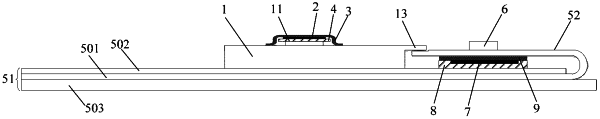
1. A flexible circuit board assembly, comprising:
a first flexible circuit board, comprising a device part provided with components;
a first wave absorbing layer, disposed on a side of the device part and configured to cover the components; and
a conductive fabric layer, disposed on a side of the first wave absorbing layer facing away from the first flexible circuit board, and configured to cover the first wave absorbing layer;
wherein an edge of the conductive fabric layer are bonded to the first flexible circuit board.