| CPC H05K 1/147 (2013.01) [G06F 3/04164 (2019.05); H05K 1/118 (2013.01); H05K 1/189 (2013.01); G02F 1/13452 (2013.01); G02F 1/1368 (2013.01); G06F 2203/04103 (2013.01); G06F 2203/04107 (2013.01); H01L 25/18 (2013.01); H01R 12/61 (2013.01); H05K 2201/09227 (2013.01); H05K 2201/09409 (2013.01); H05K 2201/10128 (2013.01); H05K 2201/10136 (2013.01); H10K 59/131 (2023.02)] | 20 Claims |
|
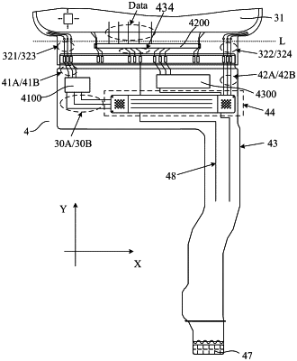
1. A display apparatus, comprising:
a display panel;
a touch layer disposed on a light-exiting surface of the display panel, the touch layer including a plurality of first touch leads and a plurality of second touch leads; and
a flexible printed circuit (FPC) bonded to the display panel, the FPC including a main FPC and a bridge FPC, wherein
the main FPC includes:
a first substrate having a first soldering region, a second soldering region and a bonding region, the bonding region being a region of the first substrate that is bonded to the display panel;
a plurality of pads disposed on the first soldering region and the second soldering region;
a touch chip disposed on the first substrate, a minimum distance between the touch chip and the first soldering region being less than a minimum distance between the touch chip and the second soldering region;
a plurality of first touch connection lines disposed on the first substrate, one end of each first touch connection line being electrically connected to the touch chip, and another end of each first touch connection line being electrically connected to a corresponding one of the plurality of first touch leads in the touch layer;
a plurality of second touch connection lines disposed on the first substrate, one end of each second touch connection line being electrically connected to a corresponding pad on the second soldering region, and another end of each second touch connection line being electrically connected to a corresponding one of the plurality of second touch leads in the touch layer; and
a plurality of third touch connection lines disposed on the first substrate, one end of each third touch connection line being electrically connected to a corresponding pad on the first soldering region, and another end of each third touch connection line being electrically connected to the touch chip; and
the bridge FPC includes:
a second substrate having a third soldering region and a fourth soldering region;
another plurality of pads disposed on the third soldering region and the fourth soldering region, a pad on the third soldering region being soldered to another corresponding pad on the first soldering region, and a pad on the fourth soldering region being soldered to a corresponding pad on the second soldering region; and
a plurality of touch transfer lines disposed on the second substrate, one end of each touch transfer line being electrically connected to a corresponding pad on the third soldering region, and another end of each touch transfer line being electrically connected to a corresponding pad on the fourth soldering region, wherein
a maximum radial dimension of any pad is less than or equal to 1.0 mm.
|