| CPC H05K 1/0298 (2013.01) [B32B 15/04 (2013.01); H01L 23/40 (2013.01); H05K 3/38 (2013.01)] | 11 Claims |
|
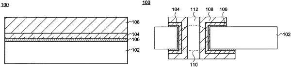
1. A wiring board comprising:
a substrate containing a first element;
a diffusion layer in contact with the substrate, the diffusion layer containing a first metal element;
a first metal film in contact with the diffusion layer, the first metal film containing a second metal element; and
a second metal film over and in contact with the first metal film,
wherein the diffusion layer has at least a region containing the first element and the first metal element and a region containing the first metal element and the second metal element,
the first metal element exists as an oxide in the diffusion layer,
the substrate has a through hole, and
the diffusion layer, the first metal film, and the second metal film continuously cover an upper surface and a lower surface of the substrate and a sidewall of the through hole.
|