| CPC H05K 1/0296 (2013.01) [H05K 1/09 (2013.01); H05K 1/181 (2013.01)] | 20 Claims |
|
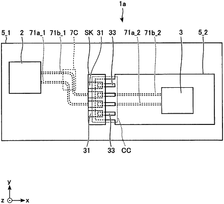
1. A printed wiring board comprising:
a substrate having an insulative property and including a first surface extending along a first plane;
a first conductor provided on the first surface of the substrate;
a second conductor provided on the first surface of the substrate and at a distance from the first conductor; and
an insulator covering a part of the first surface of the substrate, wherein
the first conductor includes: a first part extending in a first direction parallel to the first plane; a second part extending in a second direction which is parallel to the first plane and intersects with the first direction; and a third part that is connected to the first part and the second part;
the second conductor includes: a fourth part extending in the first direction; a fifth part extending in the second direction; and a sixth part that is connected to the fourth part and the fifth part;
the insulator further covers the first part, the second part, and the third part of the first conductor, and the fourth part and the fifth part of the second conductor, and
a part of the sixth part of the second conductor is exposed without being covered with the insulator.
|