| CPC H05K 1/024 (2013.01) [H05K 1/0245 (2013.01); H05K 1/0248 (2013.01); H05K 2201/0715 (2013.01)] | 20 Claims |
|
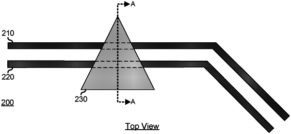
1. A printed circuit board, comprising:
a first microstrip circuit trace on an outer surface of the printed circuit board, the first microstrip circuit trace having a first straight section with a first length and configured to carry a first signal;
a second microstrip circuit trace adjacent to the first microstrip circuit trace on the outer surface, the second microstrip circuit having a second straight section with a second length longer than the first length and configured to carry a second signal; and
a patterned dielectric material applied over a first portion of the first straight section to delay the first signal relative to the second signal.
|