| CPC H05B 45/50 (2020.01) [H02M 3/337 (2013.01); H05B 41/2806 (2013.01); H05B 45/325 (2020.01); H05B 45/38 (2020.01); H05B 45/39 (2020.01)] | 7 Claims |
|
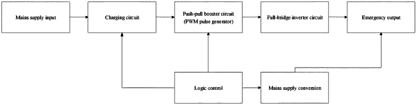
1. An emergency output circuit for starting LED lamp tubes with leakage protection, comprising a charging circuit, a push-pull booster circuit provided with a PWM pulse generator, and a full-bridge inverter circuit, wherein the charging circuit is connected to the PWM pulse generator, and the PWM pulse generator comprises a PWM chip; when a control terminal detects a power outage, a high level of voltage is instantly output to the PWM chip, and the PWM chip outputs complementary drive PWM rectangular waves with a controllable dead time to the push-pull booster circuit through two output pins; the push-pull booster circuit boosts and rectifies the rectangular waves into a 250V DC voltage and outputs the 250V DC voltage to the full-bridge inverter circuit; and the full-bridge inverter circuit comprises an inverter and a correction circuit, and the 250 VDC voltage output by the push-pull booster circuit is processed by the correction circuit in the full-bridge inverter circuit to output a stable 135V AC voltage;
wherein the inverter comprises a first NMOS transistor set and a second NMOS transistor set which are turned on alternately, the first NMOS transistor set comprises a first NMOS transistor and a second NMOS transistor, and the second NMOS transistor set comprises a third NMOS transistor and a fourth NMOS transistor; when the first NMOS transistor set is turned on, a current is output from a positive pole of a 250V DC power supply, passes through the first NMOS transistor to reach a live wire of an LED tube with leakage protection, an internal drive power supply of the LED lamp tube with leakage protection, a null wire of the LED tube with leakage protection, then reaches the second NMOS transistor, and finally returns to a negative pole of the power supply; and when the second NMOS transistor set is turned on, a current is output from the positive pole of the 250 DC power supply, passes through the third NMOS transistor to reach the null wire of the LED lamp tube with leakage protection, the internal drive power supply of the LED lamp tube with leakage protection and the live wire of the LED lamp tube with leakage protection, then reaches the fourth NMOS transistor, and finally returns to the negative pole of the power supply;
wherein the correction circuit comprises a first voltage dividing unit, a time compensation unit and an internal operational amplifier chip; and after the 250V DC voltage is divided by the first voltage dividing unit, the time compensation unit is used for time compensation of a first input terminal of the internal operational amplifier chip for processing; and
wherein the correction circuit further comprises a second voltage dividing unit, and a preset voltage output to the correction circuit is divided by the second voltage dividing unit and is then input to a second input terminal of the internal operational amplifier chip.
|