| CPC H05B 45/30 (2020.01) [H05B 41/38 (2013.01); H05B 47/10 (2020.01)] | 15 Claims |

|
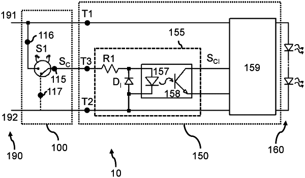
1. A LED driver control circuit arranged to generate a control signal for a plurality of LED drivers connectable to a three-phase input comprising three different phase wires each carrying an alternating current signal of a same frequency and a different phase, the LED driver control circuit comprising:
a switch adapted to controllably connect a switch output node at different times between a first switch input node and a second switch input node, a voltage of the switch output node defining the control signal;
a first voltage control circuit arranged to be connected between at least one phase wire of the three-phase input and the first switch input node and arranged to control a voltage at the first switch input node; and
a second voltage control circuit arranged to be connected to the second switch input node and to at least one phase wire of the three-phase input and arranged to control a voltage at the second switch input node,
wherein the first and second voltage control circuits are configured so that either:
the voltage at the first switch input node is greater than an instantaneous voltage of each alternating current signal for a portion of the cycle of each respective alternating current signal and the voltage at the second switch input node is no greater than an instantaneous voltage of any alternating current signal at any point during the cycle of each respective alternating current signal; or
the voltage at the first switch input node is less than an instantaneous voltage of each alternating current signal for a portion of the cycle of each respective alternating current signal and the voltage at the second switch input node is no less than an instantaneous voltage of any alternating current signal at any point during the cycle of each respective alternating current signal.
|