| CPC H04N 25/767 (2023.01) [H01L 21/3205 (2013.01); H01L 21/768 (2013.01); H01L 21/76898 (2013.01); H01L 23/481 (2013.01); H01L 27/0928 (2013.01); H01L 27/14621 (2013.01); H01L 27/14634 (2013.01); H01L 27/14636 (2013.01); H01L 27/1469 (2013.01); H04N 23/54 (2023.01); H04N 23/57 (2023.01); H04N 25/40 (2023.01); H04N 25/76 (2023.01); H01L 27/14618 (2013.01); H01L 27/1464 (2013.01); H01L 27/14641 (2013.01); H01L 27/14645 (2013.01); H01L 2224/48463 (2013.01); H01L 2224/73257 (2013.01)] | 20 Claims |
|
1. A solid-state imaging apparatus, comprising:
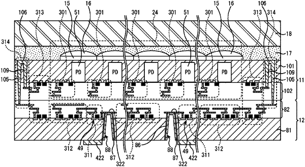
a first substrate including a pixel layer and a first wiring layer electrically connected to one another, the pixel layer including a pixel array unit with pixels for performing photoelectric conversion, wherein the first substrate includes a first bonding layer;
a second substrate including a second wiring layer including at least one output circuit to output pixel signals from the pixels and a second bonding layer; and
a first terminal to electrically connect the at least one output circuit to an external device,
wherein the first terminal is external to the second substrate and provided off-centered with respect to a central opening portion of a through hole via electrically connected to the at least one output circuit,
wherein the at least one output circuit is provided lateral to and nonoverlapping with the through hole via,
wherein the through hole via penetrates the second wiring layer and penetrates through a surface of the second substrate opposite to the second wiring layer,
wherein, in the first substrate, at least part of a drive unit to drive the pixels is formed around the pixel array unit as a pixel peripheral circuit region in a cross-sectional view, and
wherein the at least one output circuit is a plurality of output circuits.
|