| CPC H04N 25/621 (2023.01) [H04N 25/702 (2023.01); H04N 25/77 (2023.01)] | 20 Claims |
|
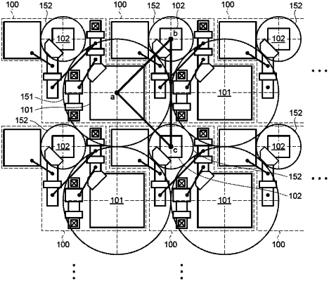
1. A light detecting device, comprising:
a first photoelectric conversion region disposed in a substrate;
a second photoelectric conversion region disposed in the substrate, wherein in a first cross-sectional view the second photoelectric conversion region is adjacent to the first photoelectric conversion region;
a third photoelectric conversion region disposed in the substrate, wherein the third photoelectric conversion region is adjacent to the first photoelectric conversion region in the first cross-sectional view;
a first trench disposed between the first photoelectric conversion region and the second photoelectric conversion region in the first cross-sectional view;
a second trench disposed between the first photoelectric conversion region and the third photoelectric conversion region in the first cross-sectional view;
a first light-blocking film disposed over the first trench in the first cross-sectional view; and
a second light-blocking film disposed over the second trench in the first cross-sectional view;
wherein an area of the first photoelectric conversion region is greater than an area of the second photoelectric conversion region in the first cross-sectional view,
wherein an area of the first photoelectric conversion region is greater than an area of the third photoelectric conversion region in the first cross-sectional view,
wherein a center portion of the first light-blocking film is disposed between a center portion of the first photoelectric conversion region and a center portion of the first trench in the first cross-sectional view, and
wherein a center portion of the second light-blocking film is disposed between the center portion of the first photoelectric conversion region and a center portion of the second trench in the first cross-sectional view.
|