| CPC H04N 25/57 (2023.01) [H01L 27/14612 (2013.01)] | 16 Claims |
|
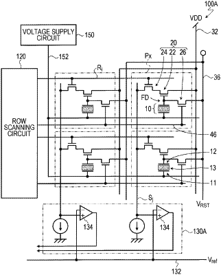
1. An imaging device comprising:
a pixel that includes:
a photoelectric converter that converts light into a charge;
a charge accumulation region to which the charge is input; and
an amplifier transistor that includes a gate electrically connected to the charge accumulation region, the amplifier transistor being configured to output a signal that corresponds to a potential of the charge accumulation region; and
a detection circuit that is configured to detect a level of the signal from the amplifier transistor, wherein
a sensitivity of the pixel is increased by varying a bias voltage applied to the pixel, when the level detected by the detection circuit is greater than a first threshold value, and
when the level detected by the detection circuit is greater than the first threshold value in a first frame, the sensitivity of the pixel is increased for a second frame after the first frame.
|