| CPC H04N 23/631 (2023.01) [H01L 27/14605 (2013.01); H01L 27/14607 (2013.01); H01L 27/14616 (2013.01)] | 20 Claims |

|
1. An imaging device comprising:
a pixel block; and
a first circuit,
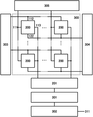
wherein the pixel block comprises a plurality of pixels arranged in a matrix,
wherein the pixel block is electrically connected to the first circuit,
wherein each of the plurality of pixels comprises a photoelectric conversion device, a first transistor, a second transistor, a third transistor, a first capacitor, a second capacitor, a first conductive layer and a second conductive layer,
wherein the photoelectric conversion device, the first transistor, the second capacitor and the first conductive layer are formed in a first layer,
wherein the first capacitor and the second conductive layer are formed in a second layer,
wherein the second layer is bonded to the first layer,
wherein the second conductive layer is bonded to the first conductive layer,
wherein one of a source and a drain of the first transistor is electrically connected to one of electrodes of the photoelectric conversion device,
wherein the other of the source and the drain of the first transistor is electrically connected to one of electrodes of the first capacitor via the first conductive layer and the second conductive layer,
wherein one of electrodes of the second capacitor is electrically connected to one of electrodes of the first capacitor via the first conductive layer and the second conductive layer,
wherein a first potential is supplied to the other electrode of the second capacitor,
wherein one of a source and a drain of the second transistor is electrically connected to the other electrode of the first capacitor,
wherein a gate of the third transistor is electrically connected to the other of the source and the drain of the first transistor,
wherein each of the plurality of pixels is configured to generate first data, wherein each of the plurality of pixels is configured to multiply the first data to have a given magnification to generate second data,
wherein the first circuit is configured to generate third data corresponding to a total of the first data generated by the plurality of pixels,
wherein the first circuit is configured to add a potential corresponding to a total of the second data generated by the plurality of pixels to the third data by capacitive coupling to form fourth data, and
wherein the first data and the second data each have an analog value.
|