| CPC H04N 13/254 (2018.05) [G01S 17/894 (2020.01); H04N 13/271 (2018.05); H04N 25/46 (2023.01); H04N 25/70 (2023.01); H04N 25/75 (2023.01); G01S 7/4914 (2013.01); G01S 7/493 (2013.01); G01S 17/36 (2013.01); G01S 17/48 (2013.01)] | 24 Claims |
|
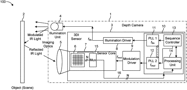
1. A time-of-flight (ToF) image sensor system, comprising:
an illumination source configured to generate a modulated light signal;
a photodetector pixel array comprising a plurality of actual pixel lines and a plurality of actual pixel columns, wherein each pixel of the photodetector pixel array is configured to receive the modulated light signal reflected from an object as a reflected modulated light signal and to demodulate the reflected modulated light signal to generate an electrical signal;
a plurality of analog-to-digital converters (ADCs), wherein each ADC of the plurality of ADCs is coupled to at least one assigned pixel of the photodetector pixel array and is configured to convert a corresponding electrical signal generated by the at least one assigned pixel into an actual pixel value and output a plurality of actual pixel values;
a binning circuit coupled to the plurality of ADCs for receiving the plurality of actual pixel values therefrom, wherein the binning circuit is configured to generate at least one interpolated pixel, wherein the binning circuit is configured to generate each interpolated pixel of the at least one interpolated pixel based on actual pixel values of the plurality of actual pixel values corresponding to a plurality of adjacent pixels of the photodetector pixel array, and wherein each interpolated pixel of the at least one interpolated pixel has a virtual pixel value,
wherein the binning circuit comprises a plurality of arithmetic logic units (ALUs) coupled to the plurality of ADCs,
wherein each ALU of the plurality of ALUs is coupled to a different group of ADCs of the plurality of ADCs for receiving the actual pixel values therefrom and is configured to combine the actual pixel values to generate a different one of the at least one interpolated pixel; and
an output circuit coupled to the binning circuit for receiving each virtual pixel value therefrom and configured to output the virtual pixel value of each of the at least one interpolated pixel according to an image structure comprising a plurality of output pixels arranged in an image pixel array.
|