| CPC H03K 5/13 (2013.01) [G06F 13/1689 (2013.01); G11C 7/1066 (2013.01); G11C 7/1093 (2013.01); G11C 7/22 (2013.01); G11C 29/022 (2013.01); G11C 29/023 (2013.01); G11C 29/028 (2013.01); G06F 13/00 (2013.01); G06F 13/4243 (2013.01); G11C 7/04 (2013.01)] | 20 Claims |
|
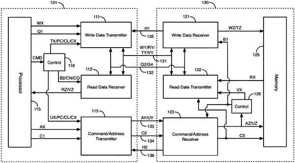
1. A memory controller to control an operation of a memory device having a plurality of memory cells, the memory controller comprising:
a first transmitter circuit to transmit data to the memory device, the data for storage in the plurality of memory cells;
a second transmitter circuit to transmit a first timing signal to the memory device, the first timing signal to time reception of the data at the memory device;
a receiver circuit to receive, from the memory device, a signal indicative of a phase comparison between a phase of the first timing signal and a phase of the data, the signal indicative of the phase comparison having a first value in response to a transition in the data leading an edge of the first timing signal, and the signal indicative of the phase comparison having a second value in response to the transition in the data lagging the edge of the first timing signal; and
a circuit to adjust, a transmit phase of data transmission by the first transmitter circuit, based on the signal indicative of the phase comparison.
|