| CPC H03K 5/05 (2013.01) [G06F 1/08 (2013.01); H03K 5/156 (2013.01); H03M 1/0624 (2013.01); H03M 1/0836 (2013.01); H03M 1/1215 (2013.01); H03M 1/82 (2013.01)] | 32 Claims |
|
1. A system, comprising:
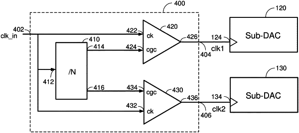
a clock dividing circuit having an input, a first output, and a second output, wherein the input of the clock dividing circuit is configured to receive an input clock signal;
a first clock gating circuit having a first input, a second input, and an output, wherein the first input of the first clock gating circuit is configured to receive the input clock signal, and the second input of the first clock gating circuit is coupled to the first output of the clock dividing circuit;
a second clock gating circuit having a first input, a second input, and an output, wherein the first input of the second clock gating circuit is configured to receive the input clock signal, and the second input of the second clock gating circuit is coupled to the second output of the clock dividing circuit;
a first sub-digital-to-analog converter (sub-DAC) having a clock input coupled to the output of the first clock gating circuit; and
a second sub-DAC having a clock input coupled to the output of the second clock gating circuit.
|