| CPC H03K 3/353 (2013.01) [H03K 5/01 (2013.01); H03K 5/023 (2013.01)] | 14 Claims |
|
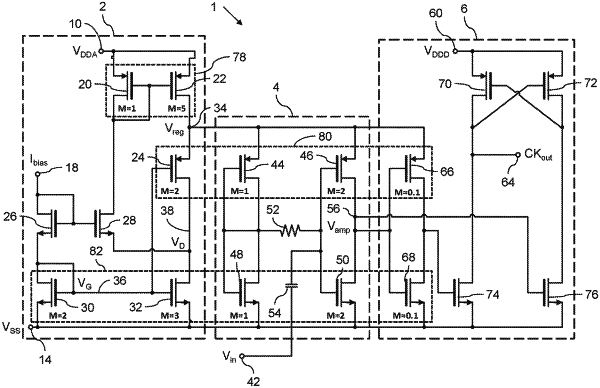
1. A circuit portion comprising:
A load circuit portion comprising a first load transistor; and
a bias circuit portion comprising:
a first replica transistor matched to the first load transistor and connected to the first load transistor at a node such that when a current flows through the first replica transistor, a current proportional to the current through the first replica transistor flows through the first load transistor;
a current input for receiving an input current;
a supply voltage input for receiving a supply voltage; and
a feedback loop arranged to:
adjust a voltage at the node connecting the first replica transistor and the first load transistor such that the first replica transistor conducts a current proportional to the input current; and
counteract variations in the voltage at the node connecting the first replica transistor and the first load transistor arising from changes in the supply voltage;
wherein the first load transistor forms part of a load inverter, the first replica transistor forms part of a replica inverter, and the replica inverter is arranged to replicate the load inverter.
|