| CPC H03K 3/0372 (2013.01) [H03K 3/012 (2013.01); H03K 19/20 (2013.01)] | 18 Claims |
|
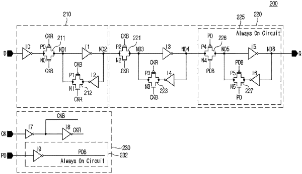
1. A retention flip-flop comprising:
a master latch configured to output a first signal generated based on a signal received from an input terminal of the master latch according to first control signals;
a slave latch comprising a retention latch, wherein the retention latch is connected directly to an output terminal of the slave latch and is configured to output a second signal generated based on the first signal input from the master latch according to the first control signals and second control signals; and
a control logic configured to: generate the first control signals based on a clock signal and provide the generated first control signals to the master latch and the slave latch, and generate the second control signals based on a power down signal and provide the generated second control signals to the slave latch,
wherein the retention latch is configured to: transmit the first signal to the output terminal as the second signal by operating as an open loop according to the second control signals during a normal operation mode, and maintain the second signal by forming a closed loop according to the second control signals during a power down mode,
wherein the slave latch comprises first circuit elements configured to: transmit the first signal inputted from the master latch to the retention latch according to the first control signals during the normal operation mode, and be powered off during the power down mode,
wherein the first circuit elements comprise:
a first transfer gate connected between an output terminal of the master latch and a first node, the first transfer gate comprising NMOS and PMOS transistors and configured to output the first signal inputted from the master latch to the first node according to the first control signals;
a first inverter connected between the first node and a second node, and configured to invert a signal of the first node and output a first inverted signal to the second node;
a second inverter configured to invert the first inverted signal of the second node and output a second inverted signal; and
a second transfer gate connected between the second inverter and the first node, the second transfer gate comprising NMOS and PMOS transistors and configured to output the second inverted signal to the first node according to the first control signals, and
wherein the retention latch is connected between the second node and the output terminal of the slave latch.
|