| CPC H03K 19/018528 (2013.01) [G06F 1/04 (2013.01); H03F 1/301 (2013.01); H03F 1/3211 (2013.01); H03F 3/45273 (2013.01); H03K 19/20 (2013.01); H04B 1/16 (2013.01)] | 20 Claims |
|
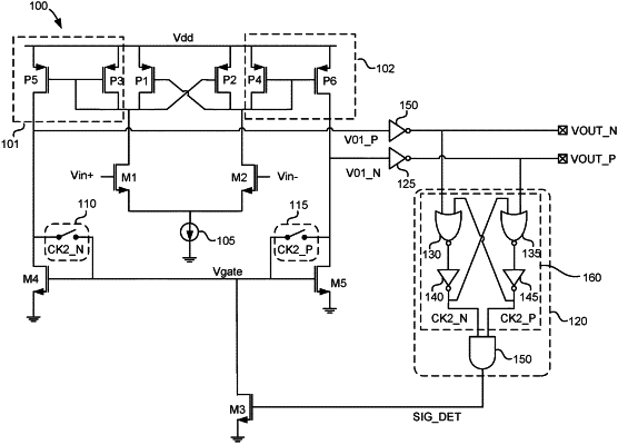
1. A low-voltage differential signaling receiver, comprising:
a differential pair of transistors configured to amplify a differential input voltage into a first differential voltage defined between a drain of a first transistor in the differential pair of transistors and a drain of a second transistor in the differential pair of transistors;
a first current mirror configured to produce a first current responsive to a drain voltage of the first transistor;
a first load transistor configured to conduct the first current to produce a first voltage, the first load transistor being selectively diode connected through a first switch;
a second current mirror configured to produce a second current responsive to a drain voltage of the second transistor; and
a second load transistor configured to conduct the second output current to produce a second voltage, the second load transistor being selectively diode connected through a second switch.
|