| CPC H03K 19/0016 (2013.01) [G06F 1/04 (2013.01); G06F 1/08 (2013.01); G06F 30/396 (2020.01); H03K 3/037 (2013.01); H03K 19/20 (2013.01)] | 11 Claims |
|
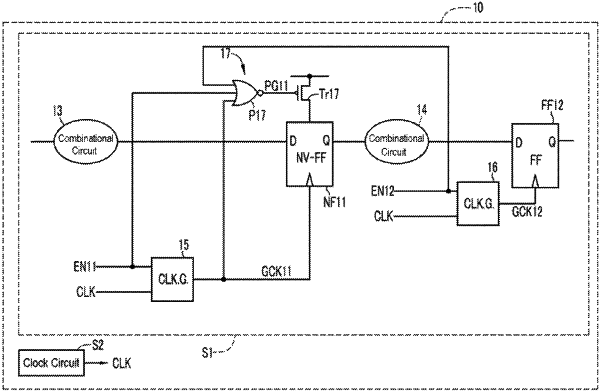
1. A semiconductor circuit device, comprising:
a first clock gating circuit configured to output a first gated clock signal generated from a clock signal, in response to a first enable signal that enables or disables the clock signal;
a non-volatile first flip-flop configured to operate in response to a clock pulse of the first gated clock signal;
an acquisition circuit, configured to acquire data inputted from the first flip-flop, directly or via a combinational circuit, according to a second enable signal that enables or disables the acquisition of the data from the first flip-flop; and
a power gating circuit including a power switch that is provided on a power source line through which electric power is supplied to the first flip-flop, the power gating circuit receiving the first enable signal and the second enable signal as power source control signals, and supplying the electric power to the first flip-flop by turning ON the power switch when the first enable signal has a logical value that enables the clock signal or when the second enable signal has a logical value that enables the acquisition of the data in the acquisition circuit.
|