|
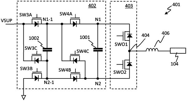
1. A switching driver for outputting an output signal to drive a transducer based on an input signal comprising: high-side and low-side supply nodes for connection to high-side and low-side voltage supplies defining an input voltage; an output node for outputting the output signal; first and second capacitor nodes for connecting a first capacitor; third and fourth capacitor nodes for connecting a second capacitor; a network of switches connected to the high-side and low-side supply nodes, the first, second, third and fourth capacitor nodes and the output node, wherein the network of switches is configured such that the switching driver can be selectively switched between any of a first set of switch states, wherein the first set of switch states comprises at least: a first switch state in which a voltage at the output node is the high-side voltage supply; a second switch state in which the voltage at the output node is the low-side voltage supply; a third switch state in which the voltage at the output node is a first positive boosted voltage which is higher than the high-side voltage supply by an amount equal to the input voltage; a fourth switch state in which the voltage at the output node is a second positive boosted voltage which is higher than the high-side voltage supply by an amount equal to twice the input voltage; and a fifth switch state in which the voltage at the output node is a first negative boosted voltage which is lower than the low-side voltage supply by an amount equal to the input voltage.
|