| CPC H03K 17/08104 (2013.01) [H03K 17/163 (2013.01); H03K 17/168 (2013.01)] | 9 Claims |
|
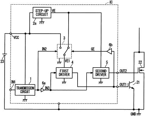
1. A semiconductor element driving circuit that drives a bipolar transistor element and a unipolar transistor element, the semiconductor element driving circuit comprising:
a transmission circuit that generates a synchronization signal synchronized with an input signal based on the input signal;
a potential generation circuit that generates a potential different from a power supply potential as a generated potential based on the power supply potential;
a first switch that selects and outputs one of the power supply potential and the generated potential as a first switch output potential, based on the synchronization signal from the transmission circuit and a delayed signal delayed from the synchronization signal, wherein the power supply potential and the generated potential are individually and simultaneously input to the first switch;
a first driver that charges a gate of the bipolar transistor element based on the synchronization signal of the transmission circuit and the first switch output potential; and
a second driver that charges a gate of the unipolar transistor element based on the synchronization signal of the transmission circuit and one of the power supply potential and the generated potential.
|