| CPC H03H 9/25 (2013.01) [H03H 3/08 (2013.01); H03H 9/02834 (2013.01); H03H 9/64 (2013.01)] | 14 Claims |
|
1. A surface acoustic wave resonator structure, comprising:
a piezoelectric substrate;
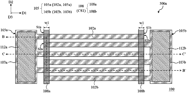
an interdigital transducer, comprising a first interdigital electrode structure and a second interdigital electrode structure, disposed side by side on the piezoelectric substrate, wherein the first interdigital electrode structure comprises first interdigital electrodes and a first interdigital electrode lead-out part connected to each other, the second interdigital electrode structure comprises second interdigital electrodes and a second interdigital electrode lead-out part connected to each other, the first interdigital electrodes and the second interdigital electrodes extend along a first direction and are alternately arranged in a second direction, the first direction and the second direction intersect with each other;
a temperature compensation layer, disposed on a side of the interdigital transducer away from the piezoelectric substrate; and
a first protection layer, disposed between the interdigital transducer and the temperature compensation layer, wherein the first protection layer is configured to protect the interdigital transducer from being oxidized; and
a clutter suppression structure, comprising a first clutter suppression layer and a second clutter suppression layer, each of which extends across the first interdigital electrodes and the second interdigital electrodes along the second direction, wherein the first clutter suppression layer and the second clutter suppression layer are arranged side by side in the first direction, and each of the first clutter suppression layer and the second clutter suppression layer is overlapped with the first interdigital electrodes and the second interdigital electrodes in a third direction perpendicular to a main surface of the piezoelectric substrate,
wherein the clutter suppression structure comprises a metal structure, and the metal structure is disposed on a side of the first interdigital electrodes and the second interdigital electrodes away from the piezoelectric substrate, and the metal structure comprises a first metal strip serving as the first clutter suppression layer and a second metal strip serving as the second clutter suppression layer;
wherein the metal structure is embedded in the temperature compensation layer, and the temperature compensation layer comprises: a first temperature compensation sublayer, disposed on a side of the first protection layer away from the first interdigital electrode structure and the second interdigital electrode structure, wherein the metal structure is disposed on a side of the first compensation sublayer away from the first protection layer; and a second temperature compensation sublayer, disposed on a side of the first temperature compensation sublayer and the metal structure away from the first protection layer; and
wherein the clutter suppression structure further comprises:
a second protection layer, disposed at least between the metal structure and the second temperature compensation sublayer to cover sidewalls of the metal structure and a surface of the metal structure at a side close to the second temperature compensation sublayer, wherein the second protection layer does not include an oxide, and the second protection layer is configured to protect the metal structure from being oxidized.
|