| CPC H03H 9/172 (2013.01) [H03H 3/02 (2013.01); H03H 9/02015 (2013.01); H03H 9/131 (2013.01)] | 18 Claims |
|
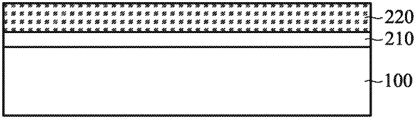
1. A bulk acoustic wave resonator, comprising:
a substrate;
a seed layer disposed on the substrate;
a bottom electrode disposed on the seed layer;
a piezoelectric layer disposed on the bottom electrode;
a top electrode disposed on the piezoelectric layer;
wherein the substrate has a cavity thereon, and the seed layer has an opening exposing a bottom surface of the bottom electrode and a portion of a bottom surface of the piezoelectric layer, and communicating with the cavity,
wherein the bulk acoustic wave resonator further comprising via holes disposed on a region of the cavity outside the bottom electrode and the top electrode, and the via holes are in communication with the cavity and the opening.
|