| CPC H03F 3/245 (2013.01) [H03F 2200/451 (2013.01)] | 19 Claims |
|
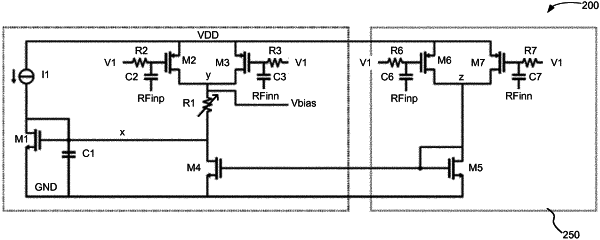
1. A bias circuit for a power amplifier, PA, the bias circuit comprising:
a first transistor having its drain terminal and its gate terminal connected to a first circuit node and its source terminal connected to a first supply terminal;
a first current source connected to the first circuit node;
a first resistor connected between the first circuit node and a second circuit node;
a second transistor configured to receive a first component of a differential input signal to the PA at its gate terminal, having its drain terminal connected to the second circuit node and its source terminal connected to a second supply terminal;
a third transistor configured to receive a second component of the differential input signal to the PA at its gate terminal, having its drain terminal connected to the second circuit node and its source terminal connected to a second supply terminal;
a fourth transistor having its gate terminal connected to a third circuit node, its drain terminal connected to the first circuit node, and its source terminal connected to the first supply terminal;
the gate terminals of the second transistor and the third transistor being configured to be biased by a first voltage; and
the bias circuit being configured to generate a bias voltage for the PA at the second circuit node.
|