| CPC H03F 1/301 (2013.01) [H01L 21/561 (2013.01); H01L 21/565 (2013.01); H01L 23/3121 (2013.01); H01L 23/3675 (2013.01); H01L 23/528 (2013.01); H01L 24/16 (2013.01); H01L 24/32 (2013.01); H01L 24/73 (2013.01); H01L 24/81 (2013.01); H01L 24/83 (2013.01); H01L 24/92 (2013.01); H01L 24/97 (2013.01); H03F 3/21 (2013.01); H01L 2224/16227 (2013.01); H01L 2224/32245 (2013.01); H01L 2224/73253 (2013.01); H01L 2224/92225 (2013.01); H03F 2200/451 (2013.01)] | 13 Claims |
|
1. A power amplifier module (PAM), comprising:
a topside;
a bottomside opposite the topside, as taken along a centerline extending through the power amplifier module;
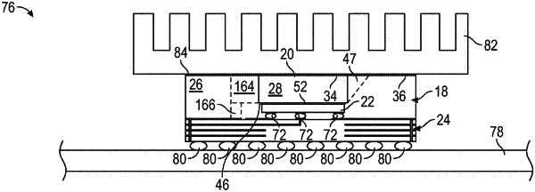
a radio frequency (RF) power die located between the topside and the bottomside taken along the centerline, the RF power die having a frontside, a backside, a frontside input/output (I/O) interface on the frontside, and a field effect transistor having a gate terminal and a drain terminal, wherein the frontside I/O interface includes a first bond pad electrically connected to the gate terminal, and a second bond pad electrically connected to the drain terminal;
a module substrate having a die support surface, an outer principal surface opposite the die support surface, an interconnection interface at the die support surface, an assembly-level interface at the outer principal surface, and electrically-conductive interconnect features that electrically couple the interconnection interface with the assembly-level interface, wherein the RF power die is mounted to the module substrate in an inverted orientation such that the frontside of the RF power die faces the die support surface of the module substrate, the interconnection interface is electrically coupled to the frontside I/O interface of the RF power die, the interconnection interface includes a first substrate interconnect feature connected to the first bond pad of the RF power die, and a second substrate interconnect feature connected to the second bond pad of the RF power die, and the module substrate is devoid of thermal vias below the RF power die;
a topside cooling interface substantially coplanar with the topside of the PAM;
a topside thermal extension having an upper surface at least partly defining the topside cooling interface of the PAM and having a lower surface in thermal contact with the backside of the RF power die;
a molded module body surrounding the RF power die and peripherally surrounding the topside thermal extension, wherein the molded module body is molded onto the die support surface of the module substrate and entirely covers the die support surface, and wherein the topside thermal extension extends from a location adjacent the RF power die in a direction opposite the module substrate to breach an upper surface of the molded module body; and
a primary heat extraction path extending from the backside of the RF power die to the topside cooling interface of the PAM in a direction opposite the module substrate.
|