| CPC H03F 1/0205 (2013.01) [H03F 3/217 (2013.01); H03F 2200/03 (2013.01)] | 20 Claims |
|
1. A class-D driver circuit, comprising:
an input terminal;
an output terminal;
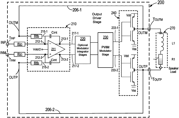
an input integrator stage having an amplifier with an input node and an output node, the input node coupled to the input terminal through an input resistor to receive an input signal;
a feedback path coupling the input node to the output terminal through a feedback resistor and an integration capacitor to receive a feedback current, the integration capacitor coupled between the input node and the output node of the amplifier, the input integrator stage configured to produce a filtered input signal at the output node;
a switched modulator stage coupled to the input integrator stage and configured for receiving the filtered input signal from the input integrator stage and generating a control signal;
an output driver stage coupled to the switched modulator stage and configured to receive the control signal for driving an output transistor and to provide an output signal at the output terminal; and
a compensation circuit including an inverter and a switched resistor coupled between the output terminal of the class-D driver circuit and the output node of the input integrator stage, wherein the compensation circuit is configured to provide a compensation current whose magnitude matches the magnitude of the feedback current.
|