| CPC H03B 28/00 (2013.01) [G06F 1/022 (2013.01); H03H 9/19 (2013.01); H03B 2200/0034 (2013.01)] | 10 Claims |
|
1. A circuit device comprising:
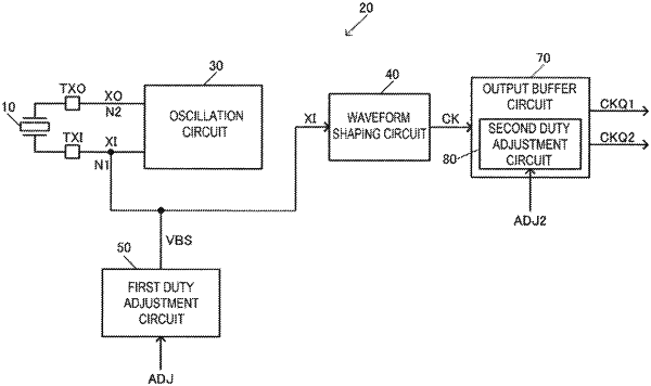
an oscillation circuit which is electrically coupled to a first node to electrically be coupled to one end of a resonator and a second node to electrically be coupled to another end of the resonator, and is configured to oscillate the resonator to generate an oscillation signal;
a waveform shaping circuit which is coupled to the first node, to which the oscillation signal is input from the first node, and which is configured to output a clock signal obtained by performing waveform shaping on the oscillation signal;
a first duty adjustment circuit configured to perform a duty adjustment of the clock signal; and
an output buffer circuit configured to output a first output clock signal and a second output clock signal to an outside based on the clock signal, wherein
the output buffer circuit includes a second duty adjustment circuit configured to perform a duty adjustment of the second output clock signal, and
the second duty adjustment circuit includes:
a reference inverter circuit configured to output a signal obtained by buffering the clock signal to an output node; and
a duty adjusting inverter circuit which is coupled in parallel to the reference inverter circuit, and is configured to output the signal obtained by buffering the clock signal to the output node.
|