| CPC H02M 7/219 (2013.01) [H02J 50/001 (2020.01); H02J 50/20 (2016.02)] | 20 Claims |
|
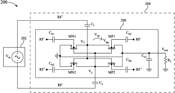
1. A complementary metal-oxide semiconductor (CMOS) rectifier for use in radio frequency (RF) energy harvesting, comprising:
an energy harvesting antenna configured to receive an electromagnetic radiation and generate an oscillating current, wherein the oscillating current is an RF+ positive current during a first half cycle and is an RF− negative current during a second half cycle;
a first rectifier stage including:
a first energy harvesting capacitor C1 connected to the RF+ positive current;
a second energy harvesting capacitor C2 connected to the RF− negative current;
a cross coupled CMOS circuit connected to the antenna, wherein the cross coupled CMOS circuit includes:
a first output capacitor Cs1 having a first stage voltage output terminal, wherein a second terminal of Cs1 is connected to a ground;
a first P-channel metal oxide semiconductor (PMOS) transistor MP1 connected at its drain to the first energy harvesting capacitor C1, at its source to the first stage voltage output terminal and at its gate to the second energy harvesting capacitor C2;
a first N-channel metal oxide semiconductor (NMOS) transistor MN1 connected at its drain to the first harvesting capacitor C1, at its source to a ground terminal and at its gate to the second energy harvesting capacitor C2;
a second PMOS transistor MP2 connected at its drain to the second energy harvesting capacitor C2, at its source to the first stage voltage output terminal and at its gate to the first energy harvesting capacitor C1;
a second NMOS MN2 connected at its drain to the second harvesting capacitor C2, at its source to the ground and at its gate to the first harvesting capacitor C1;
a first body biasing capacitor Cb1 connected between the RF− negative current and a body contact of the first NMOS transistor MN1;
a second body biasing capacitor Cb2 connected between the RF− negative current and a body contact of the first PMOS transistor MP1;
a third body biasing capacitor Cb3 connected between the RF+ positive current and a body contact of the second NMOS transistor MN2; and
a fourth body biasing capacitor Cb4 connected between the RF+ positive current and a body contact of the second PMOS transistor MP2.
|