| CPC H02M 1/0095 (2021.05) [H02M 3/07 (2013.01)] | 27 Claims |
|
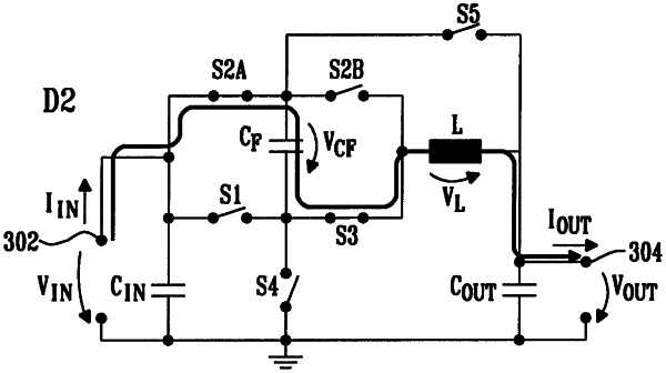
1. A power converter for providing an output voltage with a target conversion ratio, the power converter being operable in a first mode as a step-down converter or in a second mode as a step-up converter, the power converter comprising a ground port, a first port and a second port;
an inductor having a first terminal connected to the second port;
a flying capacitor coupled to a network of switches comprising
a first switch to couple a first terminal of the flying capacitor to the first port;
a second switch to couple a second terminal of the flying capacitor to the first port;
a third switch to couple the first terminal of the flying capacitor to the second terminal of the inductor;
a fourth switch to couple the second terminal of the flying capacitor to the second terminal of the inductor;
a fifth switch to couple the second terminal of the flying capacitor to the ground port;
a sixth switch to couple the first terminal of the flying capacitor to the second port; and
a driver adapted to drive the network of switches with a sequence of states during a drive period, wherein depending on the mode of operation the sequence of states comprises at least one of a first state and a second state;
wherein in the first state the ground port is coupled to the second port via a first path and a second path, the first path comprising the flying capacitor and the inductor, and the second path comprising the flying capacitor while bypassing the inductor;
wherein in the second state the first port is coupled to the second port via a third path that includes the inductor and wherein the ground port is coupled to the first port via a fourth path that includes the flying capacitor while bypassing the inductor.
|