| CPC H02M 1/0045 (2021.05) [H02M 1/0085 (2021.05); H02M 3/07 (2013.01); H02P 7/29 (2013.01); H02P 7/293 (2016.02)] | 20 Claims |
|
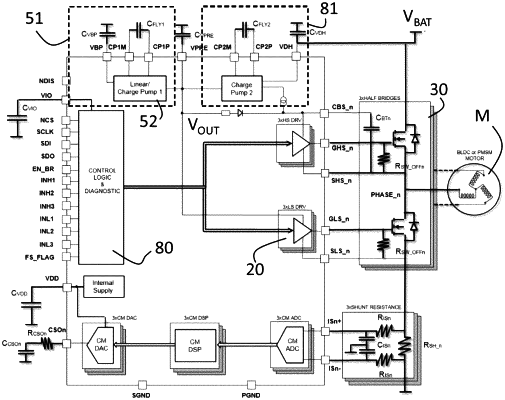
1. An electronic circuit, comprising:
an input node configured to receive an input voltage; and
a configurable voltage regulating circuit, including:
a first switch coupled between the input node and a common mode node;
a second switch coupled between said common mode node and a ground node;
a flying capacitor coupled between the common mode node and a pump node;
a third switch coupled between the input node and the pump node;
a fourth switch coupled between the pump node and an output node;
an error amplifier having a first input and a second input;
a sense resistance network coupled between the output node and the first input of the error amplifier, the sense resistance network configured to provide a sensed output voltage at the first input of the error amplifier, said error amplifier receiving a reference voltage at the second input and configured to generate an error signal;
a charging circuit configured to supply a charging current to said pump node, said charging circuit configured to control a value of said charging current as a function of said error signal; and
a switch command signal generator configured to generate respective first, second, third, and fourth switch signals to control respectively said first switch, second switch, third switch, and fourth switch,
wherein, if the input voltage is lower than a first threshold, said switch command signal generator being configured to set the configurable voltage regulating circuit as a charge pump by generating the first and second switch signals driven by opposite phases of a clock signal to couple alternatively the common mode to the input voltage and the ground, the third and fourth switch signals being driven by opposite phases of said clock signal to couple alternatively the pump node to the output node and to the charging circuit, and
if the input voltage is greater than a second threshold, said switch command signal generator being configured to set the configurable voltage regulating circuit as a linear regulator by generating the first switch signal keeping the first switch open and the second, third, and fourth switch signals keeping the second, third, and fourth switches closed.
|