| CPC H02H 9/046 (2013.01) [H02H 1/0007 (2013.01); H03K 17/0826 (2013.01); H01L 27/0248 (2013.01)] | 12 Claims |
|
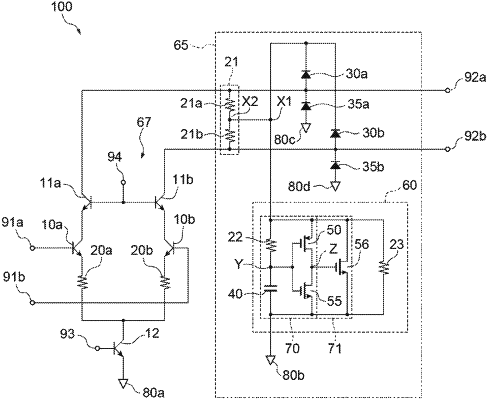
1. An electrostatic protection circuit comprising:
a first output terminal and a second output terminal;
a common node having an intermediate voltage;
a first diode connected between the first output terminal and the common node;
a second diode connected between the second output terminal and the common node;
an intermediate voltage circuit including a first dividing resistor and a second dividing resistor, the first dividing resistor being connected between the first output terminal and the common node in parallel with the first diode, the second dividing resistor being connected between the second output terminal and the common node in parallel with the second diode; and
a clamp circuit connected between the common node and a ground line, the clamp circuit being configured to electrically connect the common node to the ground line in accordance with the intermediate voltage.
|