| CPC H01S 5/11 (2021.01) [H01S 5/18305 (2013.01); H01S 5/185 (2021.01); H01S 5/34333 (2013.01)] | 28 Claims |
|
1. A light-emitting device, comprising:
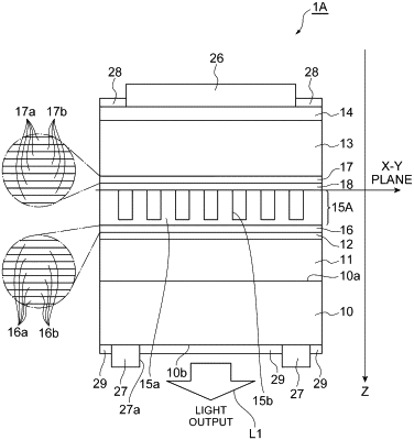
a substrate having a main surface;
a first cladding layer provided on the main surface;
an active layer provided on the first cladding layer;
a second cladding layer provided on the active layer;
a resonance mode formation layer provided between the first cladding layer and the active layer or between the active layer and the second cladding layer, the resonance mode formation layer including a base layer and a plurality of modified refractive index regions, the plurality of modified refractive index regions having a refractive index different from a refractive index of the base layer and distributed two-dimensionally on a design surface orthogonal to a normal of the main surface; and
a high refractive index layer provided between the first cladding layer and the second cladding layer, the high refractive index layer having a refractive index higher than a refractive index of any of the first cladding layer, the second cladding layer, and the resonance mode formation layer, the high refractive index layer provided in at least one of a space in which the resonance mode formation layer is sandwiched between the high refractive index layer and the active layer, and a space in which the high refractive index layer is sandwiched between the active layer and the resonance mode formation layer, wherein
the first cladding layer, the active layer, the second cladding layer, the resonance mode formation layer, and the high refractive index layer mainly contain a nitride semiconductor, and
the high refractive index layer has a superlattice structure in which two or more layers having refractive indices different from each other are repeatedly laminated along a normal direction of the main surface.
|