| CPC H01S 5/06253 (2013.01) [H01S 5/0261 (2013.01); H01S 5/0428 (2013.01); H01S 5/183 (2013.01); H01S 5/423 (2013.01)] | 25 Claims |
|
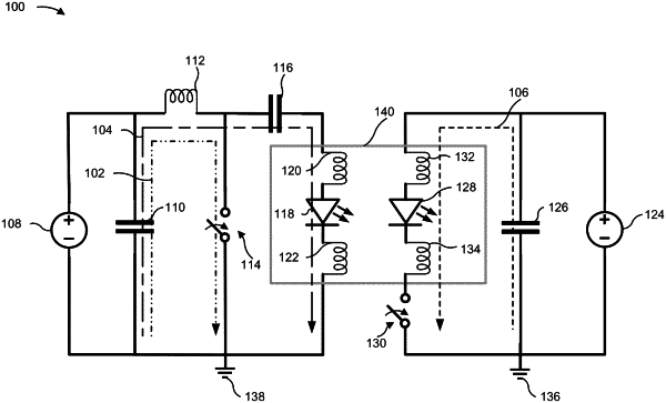
1. An electrical drive circuit for driving a multi-section optical load, the electrical drive circuit comprising:
a charging circuit path for charging, during a charging time between a first time and a second time, one or more inductive elements;
a discharging circuit path for generating, during a first time interval after the charging time, a compensation electrical pulse by discharging the one or more inductive elements; and
a main circuit path for generating, during a second time interval beginning at a third time different from the second time, a main electrical pulse,
wherein at least a portion of the first time interval overlaps with the second time interval;
wherein the electrical drive circuit is configured to:
provide the compensation electrical pulse to a compensation section of the multi-section optical load to cause the compensation section to emit a compensation optical pulse,
wherein the second time and the third time are controlled or adjusted such that an optical power of the compensation section increases to a peak power at the third time; and
provide the main electrical pulse to a main section of the multi-section optical load to cause the main section to emit a main optical pulse,
wherein the compensation electrical pulse and the main electrical pulse are both formed and provided to the multi-section optical load via independent circuit paths, and
wherein a combined optical pulse includes the compensation optical pulse and the main optical pulse such that:
a rise time of the compensation optical pulse defines a rise time of the combined optical pulse that is less than a rise time of the main optical pulse, and
a fall time of the main optical pulse defines a fall time of the combined optical pulse.
|