| CPC H01S 5/0267 (2013.01) [F21K 9/235 (2016.08); H01S 5/0261 (2013.01); H01S 5/4031 (2013.01); H01L 33/60 (2013.01)] | 20 Claims |
|
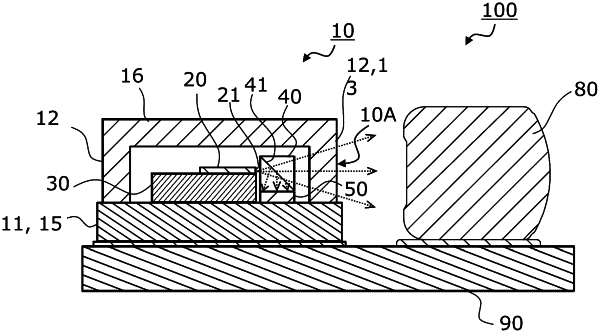
1. A light emitting device comprising:
a package having a light extraction face that has a light transmitting region, and having a base that has a mounting face;
a first light emitting element disposed on the mounting face in the package and having an emission face configured to emit divergent light, the emission face being perpendicular to the mounting face of the base;
a photodetector disposed in the package; and
an optical member disposed in the package on the photodetector, wherein the light emitted from the first light emitting element is incident on the optical member, and wherein the optical member is configured to reflect a portion of the incident light and to transmit a remainder of the incident light therethrough; wherein:
the photodetector has a light receiving face configured to receive the light emitted from the first light emitting element and reflected by the optical member; and
the light emitted from the first light emitting element and transmitted through the optical member exits from the package through the light transmitting region.
|